Visual reality check on Intel claims to being smaller and denser than the "others" ......
 this is now for ARM productsQualcomm's current 10nm chipset, the Snapdragon 835, a full function SOC with memory and all functions present inside the penny sized SOC.
  Samsung's current 10nm chipset, the Exynos 8895, a full function SOC with memory and all functions inside the smaller than a penny sized SOC.
vs
Intel's "small and light M class" CPU (still missing lots of various functions and it HAS NO BULK MEMORY as shown) Yes, Intel's two larger chipsets sitting on a daughter board still don't make up a full function SOC like the Qualcomm 835 and the Samsung Exynos 8895 shown above
 this is now for Intel x86 products
  Intel, your misleading Power Points and Press releases cannot change what is real.
 Your "technical leadership" is all past tense and getting further and further behind as the months roll on past into whole full years of "behind".
=======================================
News Flash Intel says they plan to go to 10nm, 7nm and 5nm using their existing FinFET processes. Time line stated by Intel during their lithography tech presentations this past week is 2018 for 10nm, 2020 for 7nm and 2022 for 5nm. These brown vapor announcements are running
two full years behind the others at this current time.
TSMC and Samsung have announced (and have built Apple sample runs on) a refined multi-mask EUV FinFET for 7nm for this upcoming year --- with Gate All Around (electron laser) being their production pick for 5nm and 3nm in 2019-2020.
Global Foundries announces a complete skipping of later generation 7nm FinFET processes and an early adaptation of a 5nm electron laser based Gate All Around process at 5nm and 3nm (skipping out on the 7nm generation completely as wasted capital and wasted time). This is a wise plan for Global as
Apple has already let the main contracts for 7nm to TSMC with Samsung as a production backup "safety".
ASML (the company that makes all the lithography equipment) was up on the stage with the NON-Intel groups, silently supporting the reality of what was being said as two (2) 5nm electron laser production machines are being built, with one of each slated to be installed at both TSMC and at Samsung sometimes later this year --- with Global Foundries getting their first one early of next year.
Yep, Apple invests in their product lines 3 years out with basic production process research and Apple funds one future current ASML production line at each pet vendor for their dedicated production refinement use for the next 2-3 years as they build the "at risk" early lots of iPhone chipsets.
"Read between the lines" time --- Intel is using their brown vapor cannon very freely yet again to cover the fact they HAVE NO REAL PRODUCTION LITHOGRAPHY "INNOVATION" PLANS PAST 10nm and that their current 10nm plan is shot full of nagging low yield production issues at the moment, issues that will likely take a projected 12 months to work through Intel's crop of 10nm issues.
Intel is also noted to be at the foot of the line to get the new ASML 5nm electron laser lithography equipment -- a fact that explains why Intel is sticking to finFET at 7nm, 5nm and 3nm supposedly. That puts them yet another year behind the pack when they finally get real about having to use electron laser technology.
Intel now states publicly their tick-tock cycle now takes 3-4 years to complete on a single lithography level .....


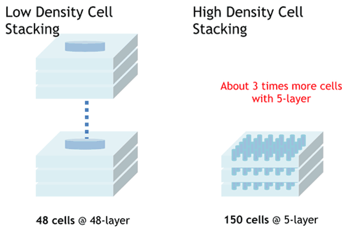
...... and yes, Intel, that is your brand new non-competitive 14nm Optane stuff shown over on the left in the pic below.
(example comes from 14nm Intel Optane vs the Besang 10nm Gate All Around system)
That Gate All Around is some powerful stuff, really ..... this comparison holds true at any future lithography level, btw ..... this comparison is made at 14nm which is the current Intel reality. 10nm, 5nm and 3nm will be even worse for Intel when that point in time rolls around. Please remember, Intel is two full years behind in lithography as of right now, so Intel's 14nm goes vs everybody else's 10nm, 10 Intel goes vs everybody else's 7 ..... by then Intel should be pretty much defunct or close to it and simply be unable to buy the new ASML technology and do the needed development to even try to catch up.

========================================
Voltage downsize plays out against aging Intel PC CMOS technologyIntel announces they are forming a "task force" to redo all PC CMOS requirements to allow all devices to run on 2 volts or less.
Intel can't buy readily buy really cheap pieces for their PC stuff any more since there is now a ever larger voltage gap between the cheaper, smaller, more efficient stuff the phone industry uses (in very large volumes) vs the old stuff what Intel x86 PC products still have to use (legacy production in much smaller volumes).
This need has arisen very recently since oncoming even more modern lithography levels run the entire shebang on 1.5 volts or less. The voltage gap has become a Grand Canyon of late .... with Intel sitting on the wrong side of the gap.
Intel still produces legacy products that run at 5 volts or more --- and Intel HAS to get with the sub 2 volt program ASAP or lose the market for those items completely to the voltage decrease which has already arrived.

