https://seekingalpha.com/article/4338843-taiwan-semiconductor-manufacturing-c...This is a finance magazine Intel fan boy searching for something good to say about Intel's far far future plans. Mind you, he does not understand the delays just put forth by Intel will be ADDING YEARS to the timelines he reports, he is just regurgitating what Intel has released in print for "Intel's far future plans".
And it is obvious someone from Intel has shared "the true meanings" of Intel's 10nm and 7nm because he quotes that propaganda as fact.
Still, taken in perspective it gives you timelines that will only get worse (with more delay) as Intel fumbles the ball time after time trying to do things that TSMC cannot pull off the very first time out of the gate ......
The precept of this article should be that Intel will buy (or rent) current TSMC style lithography going forward. Intel has said OFFICIALLY that they are going to do this, but Intel has certainly not ordered any new lithography scanners to put into TSMC to put any reality behind those empty words.
Not having ordered 2-3 year lead time ASML scanner lines several years ago means Intel has to rent 5nm production time from TSMC/Apple or Samsung. Samsung doesn't HAVE enough equipment to handle Intel's volumes, so forget Samsung as a source for more than a single chipset item or two.
Intel trying to rent enough huge massive amounts 5nm production time from TSMC/Apple is a joke right now too as all TSMC/Apple's 5nm production is booked up for up to 3 years ahead at this stage of things.
Apple paid for the original TSMC 5nm lines and Apple will not turn them loose until they are up and running on 3nm with their full current Apple production. So, 3nm will be ramping up for world-wise use before there is enough free 5nm capacity to even start to handle Intel's needed volumes.
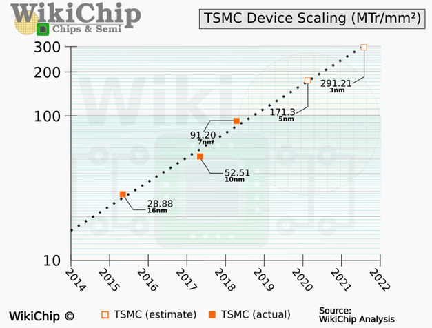
Furthermore, the bottom graph that is showing Intel making advances to lithography stages
well before TSMC does kinda loses track of the fact that Intel is having TSMC build all their advanced lithography for them going forward.
This last graph is pure optimistic Intel fanboy fiction from ages past, in other words.This article writer totally dismisses all the effects of 14 layer deep direct burn EUV lithography and what that means for large amounts of very fast on chip multi-level cache memory that AMD is currently using to their advantage. Intel knows nothing about this layered deep burn trick and it is not reflected in any of their current chipset designs. So to say that Intel just picks it up right along with gate all around chip construction techniques is just plain silly talk.
Intel has lost Jim Heller as a resource (he quit in frustration) and they have only Renchalla left now as their tech leader. Renchalla, the man who insisted that Intel go hire Keller, the guy who taught Renchalla how to do it when talking about fine feature advanced lithography.
This very last graph is pure "Intel wishes it were so" and it also assumes that there is copious amounts of free TSMC production space to plug Intel into ..... and we know that this is not the case.
OR ...... it assumes Intel can actually do 5nm followed by 3nm gate all around all in house at will, which is another joke to beat all jokes.
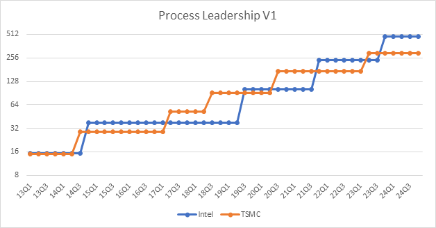 THIS LAST GRAPH IS MOSTLY BOGUS NONSENSE
So, add in a 2 year gap between the graph lines and remove all the line overlaps ---- this is closer to best case reality.
Or, simply being completely realistic, there should only be the TSMC graph line showing in the years past 2020 .....
And what is with the weird years with quarters shown on the X axis of this last graph --- this is all complete Intel Fanboy BS that was written a long long time ago, isn't it?

 Pages:

